¿¢½º·¹ÀÌ
& CT °Ë»çÀåºñ

XT V 130
¿¢½º·¹ÀÌ & CT °Ë»çÀåºñ > XT V 130

XT V 130 XT V 160 XT H MCT225

XT V 130 Electronics X-ray Inspection

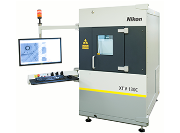
Compact, versatile and easy-to-use electronics QA system
The XT V 130C is a highly flexible and costeffective electronics and semiconductor inspection system. The system features a 130 kV/10 watt Nikon Metrology manufactured source, a globally recognized open tube design with integrated generator, and a high-resolution imaging chain.
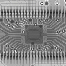
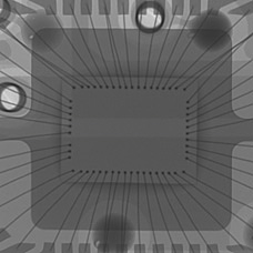
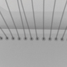
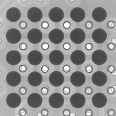
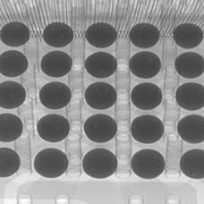
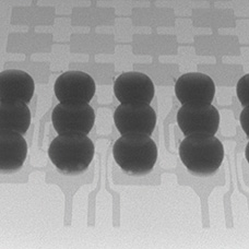
Superb image magnification enables users to zoom in on any specific item of interest
Features
  • Proprietary 20-130 kV micro-focus source with 2 ¥ìm feature recognition
  • Measurement area of 406x406 mm
  • True 75¡Æ manipulator tilting angle allows oblique viewing for easy inspection of internal features
  • A hinged door providing easy access to the inspection area
  • Serviceable components are easily accessible
Applications
  • Electronic and electrical components
    • Broken wedge bonds, lifted ball bonds, wire sweep, die attach, dry joints, bridging/shorts, voiding, BGA, etc.
  • Populated and unpopulated PCBs
    • View surface mount defects i.e. misaligned devices, solder joint porosity and bridging
    • Detailed inspection of vias, through-hole plating and multi-layer alignment
    • Wafer-level chip scale packages (WLCSP)
    • BGA and CSP inspection
    • Non-lead solder inspection
  • Micro-electro-mechanical systems (MEMS, MOEMS)
  • Cables, harnesses, plastics and many more
Benefits
  • On-line operation with intuitive joystick navigation
  • Low-cost maintenance with open-tube technology
  • Safe system requiring no special precautions or batches
  • Small footprint and low-weight for easy installation
  • CT option possible
Related solutions
  • XT V 160
  • Inspect-X
Tilt angles up to 75¡Æ offers sufficient flexibility to trace connectivity issues quickly